 |
|
You are here: Panda Wiki>Mvd Web>MvdDevelop>BN-TS>Sens-StripCIS1 (2013-03-25, TommasoQuagli)Edit Attach
PANDA CIS Sensors
Review of the properties of the PANDA strip sensors:| General properties | |
|---|---|
| wafer material | FZ Si, 4'', n/P |
| thickness | 285 ± 10 µm |
| resistivity | 2.3 ... 5.0 kΩ · cm |
| n-side isolation | p-spray |
| guard rings | 8, on p-side |
| stereo angle | 90° |
| Corners | |
|---|---|
| passive rim (including guard rings, excluding bias) | 750 µm |
| bias ring | 110 µm |
| limit active area | 860 µm |
| Pad | Distance from chip rim | Distance from active area limit |
|---|---|---|
| DC pad | 1361 µm | 500 µm |
| AC pad row 1 | 2861 µm | 2000 µm |
| AC pad row 2 | 3661 µm | 2800 µm |
| AC pad row 3 | 6861 µm | 6000 µm |
| AC pad row 4 | 7661 µm | 6800 µm |
- Schematic drawing of the strip sensors (click to view larger):
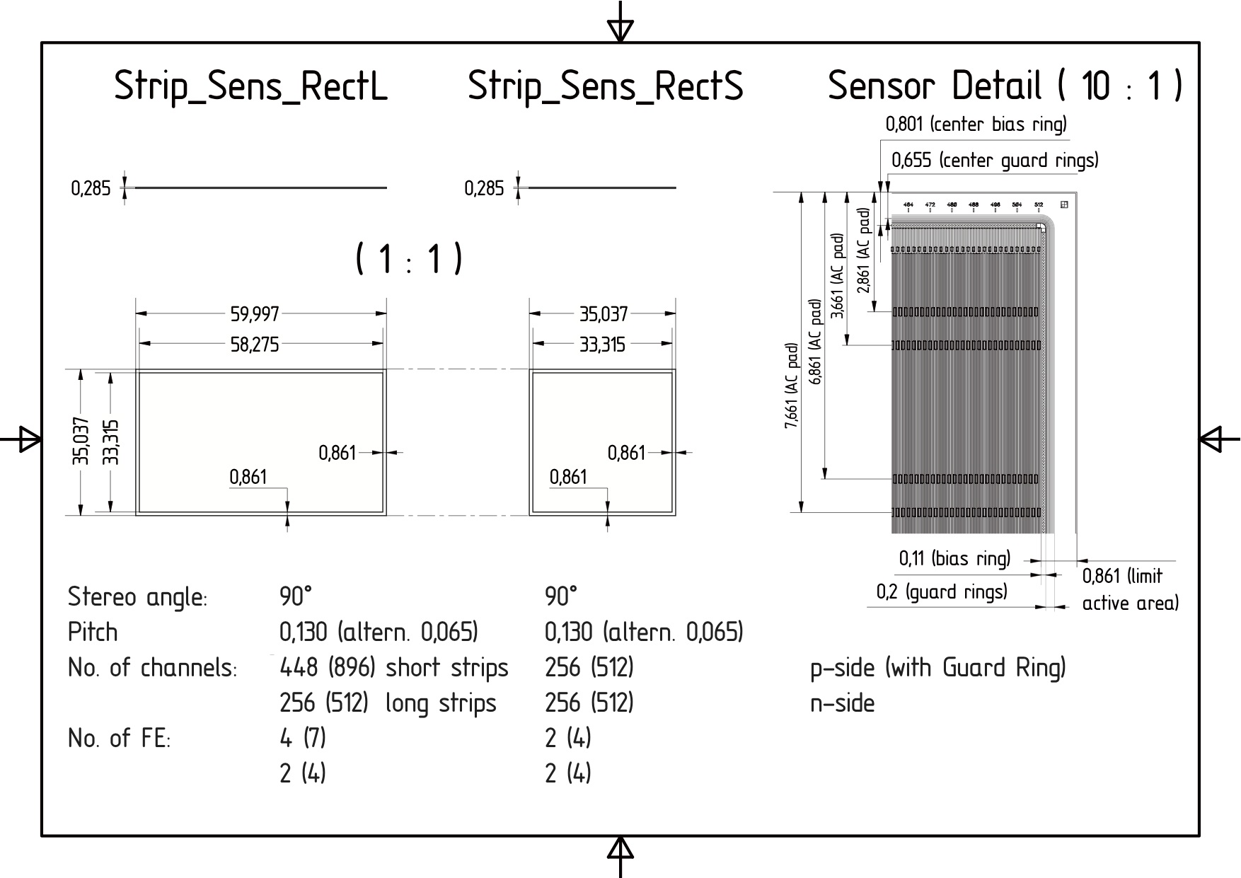
| S1 / Spssdb65 | |
|---|---|
| n-side strips | 512 (long) |
| p-side strips | 896 (short) |
| pitch | 65 µm |
| active area | 58.275 × 33.315 mm2 |
| S2 / Spssdm65 | |
| n-side strips | 512 |
| p-side strips | 512 |
| pitch | 65 µm |
| active area | 33.315 × 33.315 mm2 |
| S3 / Spssdm50 | |
| n-side strips | 384 |
| p-side strips | 384 |
| pitch | 50 µm |
| active area | 19.230 × 19.230 mm2 |
| S4 / Spssds65 / s65 "Baby" | |
| n-side strips | 128 |
| p-side strips | 128 |
| pitch | 65 µm |
| active area | 8.355 × 8.355 mm2 |
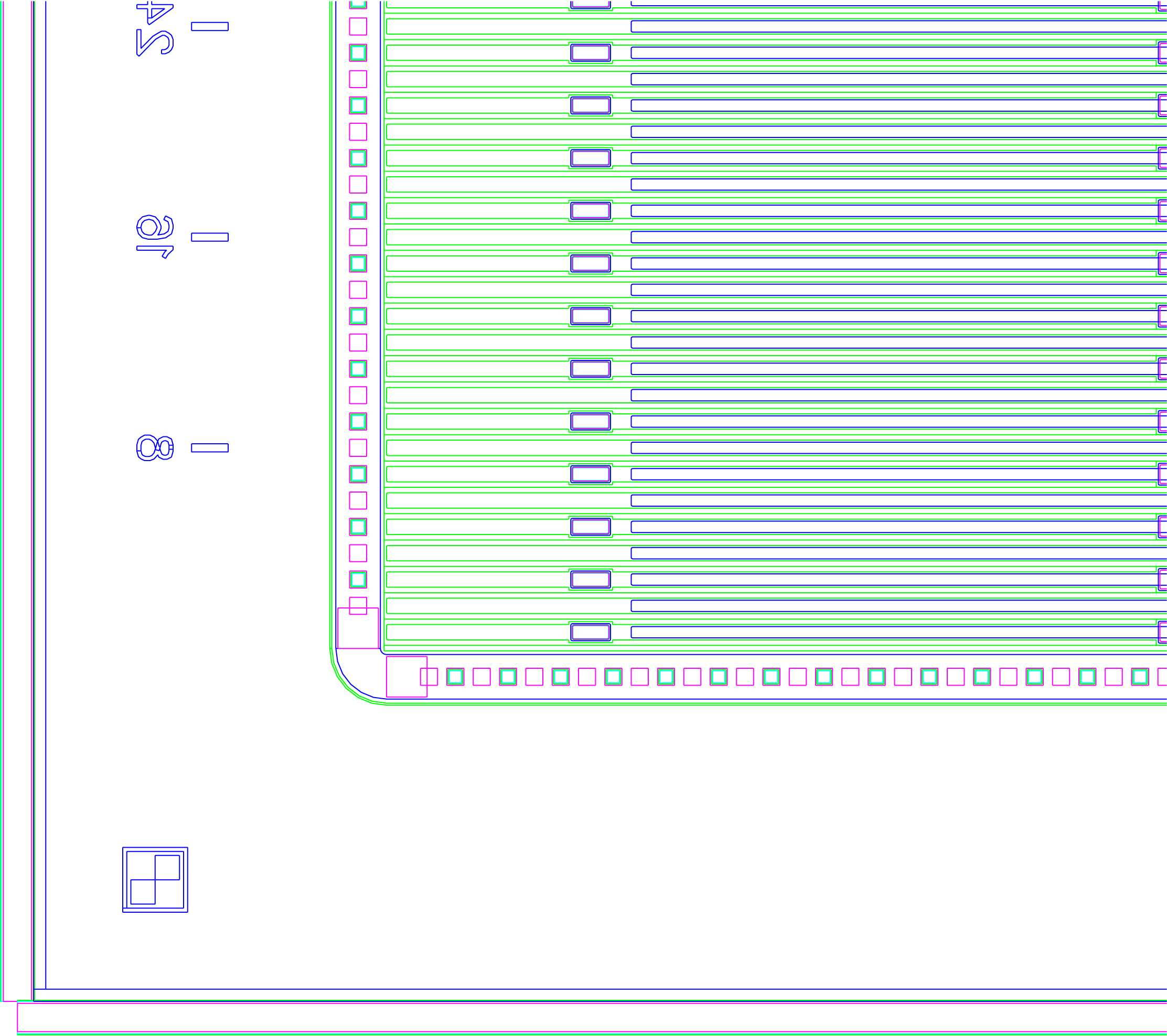
- Corner of the sensor (n-side):

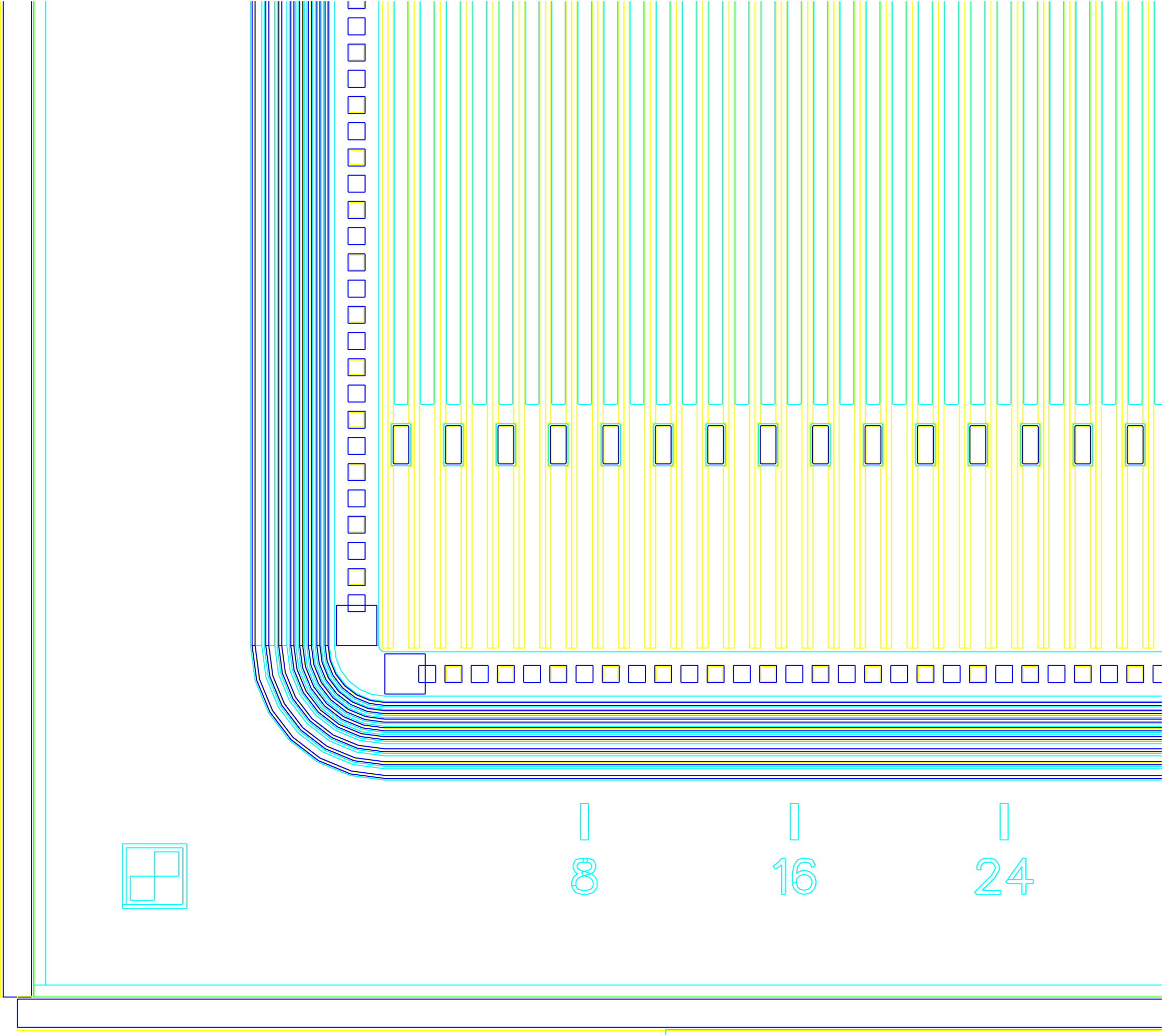
- Corner of the sensor (p-side):


| I | Attachment | Action | Size | Date | Who |
Comment |
|---|---|---|---|---|---|---|
| |
cisreportsmall.pdf | manage | 250 K | 2012-12-19 - 15:23 | UnknownUser | CIS report on PANDA sensors |
| |
schematicsensors.jpg | manage | 272 K | 2013-03-25 - 14:07 | UnknownUser | Schematic drawing of the strip sensors |
| |
sensorn_side.png | manage | 59 K | 2012-09-27 - 17:39 | UnknownUser | Sensor n-side |
| |
sensorp_side.png | manage | 87 K | 2012-09-27 - 17:41 | UnknownUser | Sensor p-side |
Edit | Attach | Print version | History: r6 < r5 < r4 < r3 | Backlinks | View wiki text | Edit wiki text | More topic actions
Topic revision: r6 - 2013-03-25, TommasoQuagli
Mvd Web
Web Home | Search Changes | Notifications Index | Topics
Web Home | Search Changes | Notifications Index | Topics
- Webs
- Cerenkov * Cerenkov.Pandacerenkov * DCS * Daq * Daq.Pandadaq * Detector * EMC * EMPAnalysis * Forwardstraws * GEM * MC * Magnet * Main * Mvd * PANDAMainz * PWA * Pbook * Personalpages * Physics * Physics.Baryons * Physics.CharmoniumAndExotics * Physics.HadronsInNuclei * Physics.OpenCharm * PhysicsCmt * SPC * STT * Sandbox * ScrutinyGroup * Tagpid * Tagpid.Pandatagpid * Tagtrk * Tagtrk.Pandatagtrk * Target * Target.ClusterJetTarget * Tof * WebServices * YoungScientists * ZArchives
Create personal sidebar
Copyright © by the contributing authors. All material on this collaboration platform is the property of the contributing authors.
Ideas, requests, problems regarding Panda Wiki Send feedback | Imprint | Privacy Policy (in German)
Ideas, requests, problems regarding Panda Wiki Send feedback | Imprint | Privacy Policy (in German)